PRODUCTS >> RAN Acceleration
5G RAN FEC Acceleration IP
Hyperscale your 5G NR RAN with Tannera’s cloud native FEC acceleration - plug & play, power efficient, scalable, and flexible solution.
Tannera’s 5G RAN FEC Acceleration IP offloads compute-intensive tasks from vRAN physical layer SW by achieving maximum performance with minimum hardware footprint. The IP includes FEC and it can be configured to use standardized DPDK/BBDEV or custom interfaces. The solution is scalable and portable, such that it can target a wide range of PCIe accelerator cards or programmable SoCs. Furthermore, the pure RTL nature of the design enables targeting ASIC solutions. With a proven power efficiency, flexibility, and speed, the Tannera’s 5G RAN FEC Acceleration IP is a market-leading lookaside acceleration solution for 5G.
Cloud native
runs in container, virtual machine, or bare metal solutions,
supports SR-IOV, VFIO, container orchestration, and other virtualization technologies,
deployable on already available PCIe FPGA resources
Fully interoperable
high bandwidth systems for the highest spectral efficiency,
plug and play integration with DPDK/BBDEV driver,
entirely in line with O-RAN AAL,
optional customizable interfaces for specific customer needs
Maximized and flexible throughput
breaking the limits and saturates the PCIe throughput,
over 200 Gbps downlink and 25 Gbps uplink throughput with PCIe Gen4 cards,
uplink centric, downlink centric or anything in between
Deployable to PCIe FPGA cards, SoC FPGA platforms, or ASIC SoCs
Fully compliant with 5G NR standard (3GPP Rel. 18, TS 38.212)
Feature rich solution providing full transport block FEC functionality
Integrated with L1 software via DPDK/BBDEV driver or using customer specific interfaces
PCIe FPGA solution is fully virtualized - supports SR-IOV, VFIO, containers/virtual machines, and container orchestration
Features the efficiency benefits of Tannera’s 5G IP cores: achieves the highest throughput for the limited hardware resources
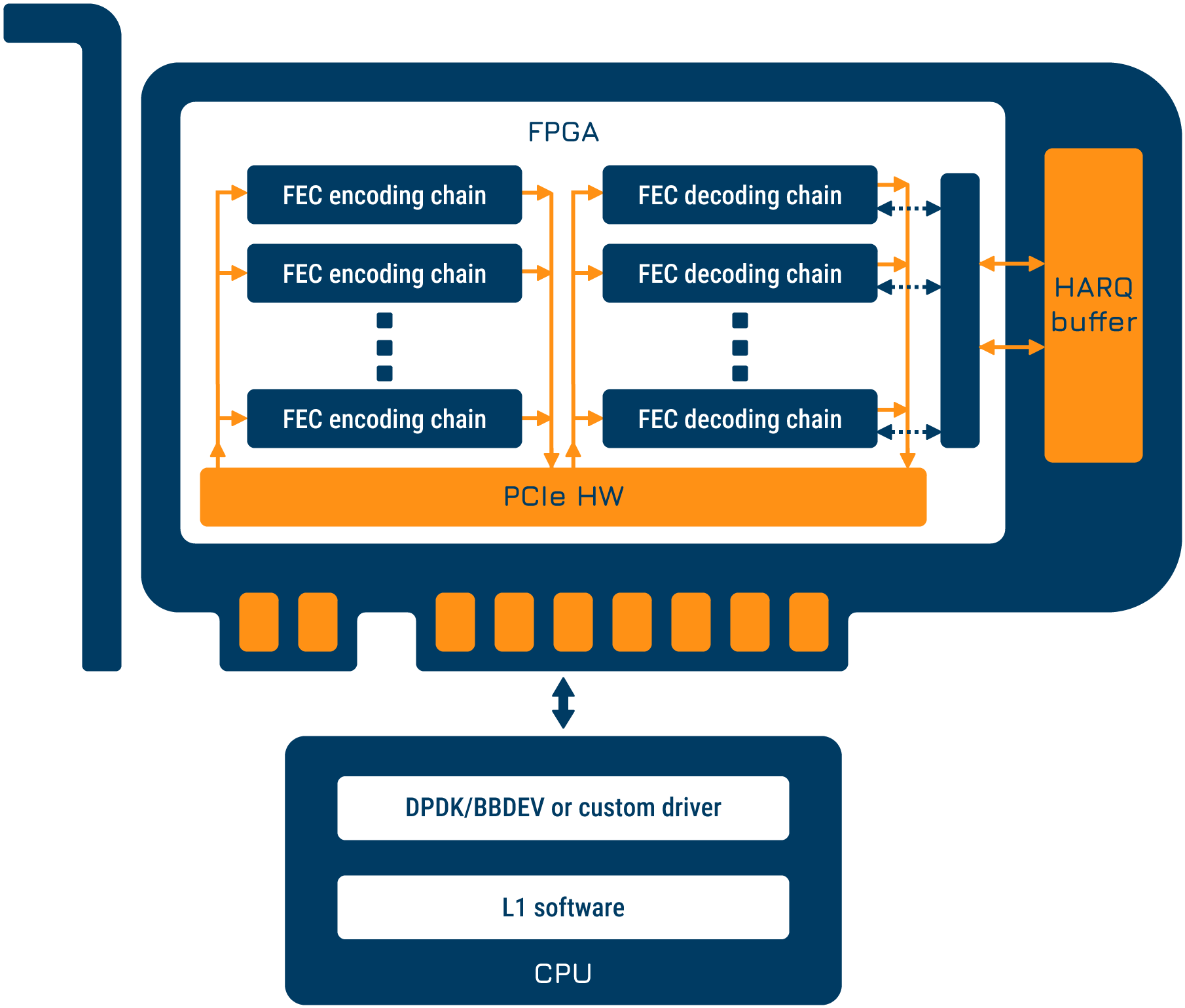
Flexible number of encoding and decoding chains in a single design
Easily customizable as per request by customer

Tannera’s 5G RAN FEC Acceleration IP offloads compute-intensive tasks from vRAN physical layer SW. Its purpose is to enable high throughput and low latency in software defined vRAN solutions.
All baseband digital processing can be done in software on server CPUs. However, the data processing in high capacity networks requires huge computing power, i.e., a huge number of CPU cores. The PCIe accelerator cards are used to run the heaviest tasks and leave the CPU free for other workload types. This way, the remaining SW workloads are performed faster, accelerating the entire vRAN. By introducing acceleration with Tannera’s 5G RAN FEC Acceleration IP, the energy consumption is drastically reduced, since a single FPGA card (consuming ~30 W) replaces hundreds of CPU cores (that may consume above 1000 W).
In small cell solutions requiring lower throughput, industry is aiming for usage of low-end CPUs or embedded CPUs, which cannot provide enough computing power for necessary 5G L1 RAN workloads. In this case, Tannera’s 5G RAN FEC Acceleration IP is used to enable the core functionalities of a small cell gNB by offloading the most intensive tasks from a CPU or to be an integral part of the entire hardware-based physical layer.
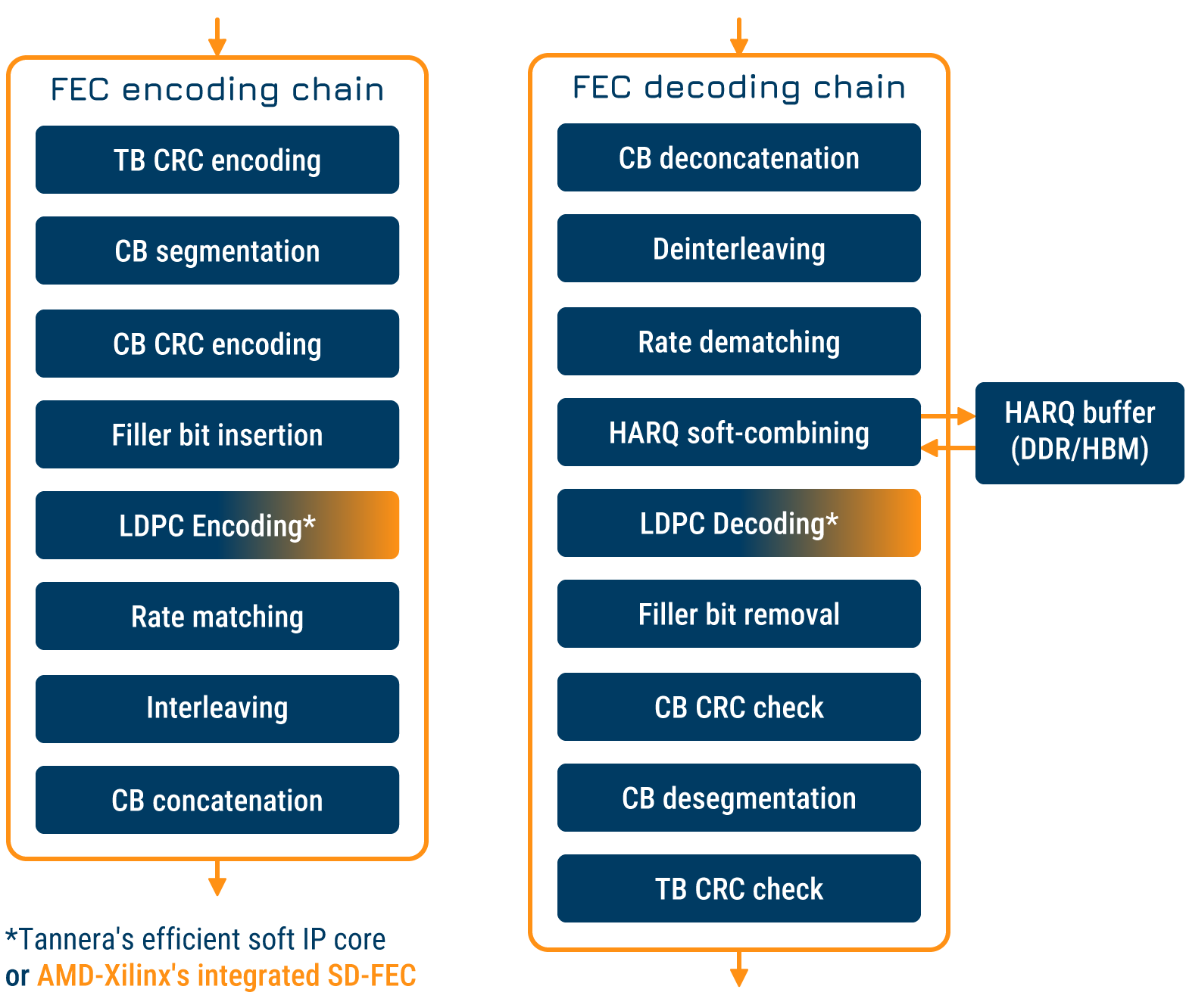
Tannera’s 5G RAN FEC Acceleration IP is fully compliant with the 5G NR standard (3GPP Rel. 18, TS 38.212) providing complete transport block FEC functionality. Depending on the deployment platform, the FEC encoding chain (downlink) and the FEC decoding chain (uplink) can use either Tannera’ efficient soft IP cores or integrated FEC IP cores already available on chip (e.g. AMD-Xilinx’s RF-SoC).

Tannera’s 5G RAN FEC Acceleration IP is a resource-efficient solution that unlocks the full potential of acceleration hardware. It consists of Tannera’s state-of-the-art IP cores that maximize the throughput, minimize the latency, and improve the spectral efficiency while using the least amount of hardware resources. Consequently, Tannera’s 5G RAN FEC Acceleration IP enables the high-end and low power acceleration even on a single device.
Tannera’s 5G RAN FEC Acceleration IP also offers flexibility in configuration for various traffic conditions (e.g. uplink-centric, downlink-centric, balanced scenarios), while keeping the PCIe throughput saturated. For example, when deployed on cards based on AMD’s FPGAs, Tannera’s acceleration solution features up to 200 Gbps of downlink and 25 Gbps uplink throughput, depending on the configuration. This makes it the highest capacity solution available on the market today.

Tannera’s 5G RAN FEC Accelerator driver enables close to theoretical throughput of PCIe bus while supporting both bare-metal and containerized solutions, as well as virtualization technologies such as SR-IOV and VFIO, thus making it a cloud native solution perfect for deployment in cloud or edge data centers.
Check out the BBDEV-compliant 5G RAN FEC Accelerator features and performance in a DEMO.
The demo shows the 5G RAN FEC Acceleration IP integrated in DPDK/BBDEV compliant PCIe accelerator. The acceleration IP is ported to AMD-Xilinx Alveo U50 FPGA acceleration card. The demo showcases throughput and virtualization capabilities.


